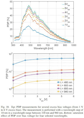
"Single-photon avalanche diodes (SPADs) have become the sensor of choice in many applications whenever high sensitivity, low noise, and sharp timing performance are required, simultaneously. Recently, SPADs designed in CMOS technology, have yielded moderately good performance in these parameters, but never equaling their counterparts fabricated in highly customized, non-standard technologies. The arguments in favor of CMOS-compatible SPADs were miniaturization, cost and scalability. In this paper, we present the first CMOS SPAD with performance comparable or better than that of the best custom SPADs, to date. The SPAD-based design, fully integrated in 180 nm CMOS technology, achieves a peak photon detection probability (PDP) of 55% at 480 nm with a very broad spectrum spanning from near ultraviolet (NUV) to near infrared (NIR) and a normalized dark count rate (DCR) of 0.2 cps/µm^2, both at 6V of excess bias. Thanks to a dedicated CMOS pixel circuit front-end, an afterpulsing probability of about 0.1% at a dead time of ∼3 ns were achieved. We designed three SPADs with a diameter of 25, 50, and 100 µm to study the impact of size on the timing jitter and to create a scaling law for SPADs. For these SPADs, a single-photon time resolution (SPTR) of 12.1 ps, 16 ps, and 27 ps (FWHM) was achieved at 6 V of excess bias, respectively. The SPADs operate in a wide range of temperatures, from -65◦C to 40◦C, reaching a normalized DCR of 1.6 mcps/µm^2 at 6 V of excess bias for the 25 µm at -65◦C."
Low Noise SPAD in 180nm Process
IEEE Journal of Selected Topics in Quantum Electronics publishes EPFL and KIST paper "A Low-noise CMOS SPAD Pixel with 12.1 ps SPTR and 3 ns Dead Time" by Francesco Gramuglia, Ming-Lo Wu, Claudio Bruschini, Myung-Jae Lee, and Edoardo Charbon.


0 Response to "Low Noise SPAD in 180nm Process"
Post a Comment