Tranlated from baidu.com: https://baijiahao-baidu-com.translate.goog/s?id=1839758590887948034&wfr=spider&for=pc&_x_tr_sl=zh-CN&_x_tr_tl=de&_x_tr_hl=de&_x_tr_pto=wapp
In-depth: Sony's three-layer CIS changes the global sensor market
Source: AI Core World (Aug 7, 2025)
Sony is developing a three-layer image sensor
Sony Semiconductor Solutions (SSS) showcased a potentially groundbreaking three-layer image sensor design as part of a presentation to investors, the company's Imaging & Sensing Solutions (I&SS) division announced today. The design promises significant performance improvements.
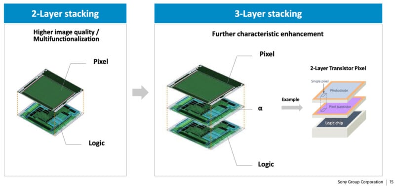
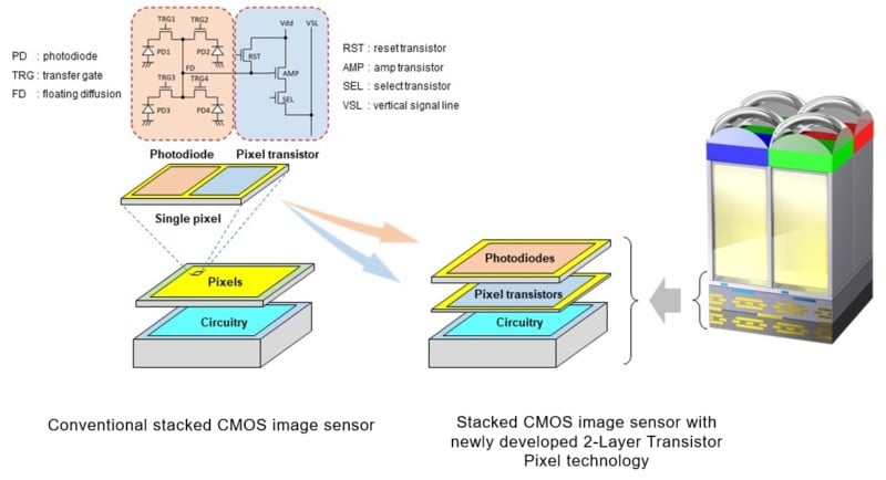
Although Sony has used stacked sensors in several cameras, including its flagship a1 II, these sensors currently have a dual-layer structure. One layer is the photodiode layer responsible for capturing light, which contains all the light-sensitive pixels; the other layer is the transistor layer located below it, which is responsible for image processing tasks. Sony's core long-term goal is to introduce the crucial third layer in the image sensor stack. This essentially means an expansion of processing power and a leap in image quality.
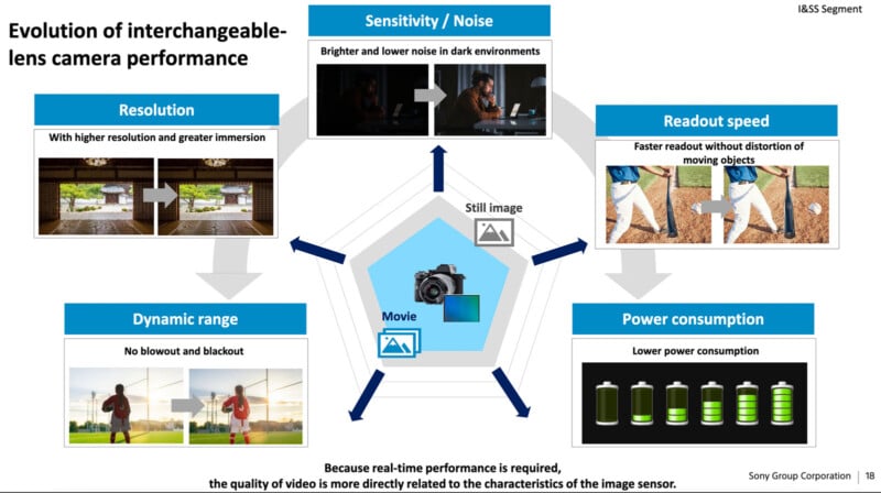
When other conditions are equal, the stronger the processing power at the sensor level, the better the imaging effect will naturally be. Sony explains that increasing processing power at the sensor level will directly translate into improvements in several key performance areas: dynamic range, sensitivity, noise performance, power efficiency, readout speed, and resolution.
While adding sensor layers doesn't directly change the pixel resolution itself, it unlocks entirely new video recording modes by significantly improving the overall speed and performance of the sensor.
Image sensors remain a core pillar of Sony's strategy in diverse areas including mobile devices, automotive, industrial and cameras. Sony expects the camera-related sensor market to continue expanding at a compound annual growth rate of 9% by fiscal 2030, which indicates that Sony will continue to increase its investment in this field.
Next-generation sensor technology will become a driving force for differentiation
Sony is focusing on R&D in multi-layer sensor stack architectures and advanced process nodes to improve sensitivity, dynamic range, power efficiency and readout speed – cutting-edge technologies that will directly power future Alpha and FX camera series. To achieve these goals, Sony plans to invest a total of nearly 930 billion yen in capital expenditures between 2024 and 2026, about half of which will be dedicated to the research and development and production of advanced image sensor processes.
As outlined in its long-term strategy, Sony is going all out and investing in next-generation sensor technologies, including multi-layer stacked image sensors.
Sony's triple-stacked sensor, used in the Xperia 1 V and adopted by other mainstream smartphone models, significantly improves image quality. The architecture also supports multimodal sensing and on-chip artificial intelligence processing, marking a shift in the industry's focus from simply pursuing resolution to intelligent sensing. The breakthrough in 22nm logic stacking technology is committed to achieving ultra-low power consumption and expanded computing power, among which FDSOI technology is expected to be applied in the field of neuromorphic sensing.
----------------------------------------------
Also covered by PetaPixel: https://petapixel.com/2025/07/30/sonys-triple-layer-image-sensor-promises-huge-performance-gains/
Sony’s Triple-Layer Image Sensor Promises Huge Performance Gains
0 Response to "Sony 3-layer stacked sensor"
Post a Comment