Link: https://www.mdpi.com/1424-8220/21/3/743
 Structure and operation of a typical Single-Photon Avalanche Diode (SPAD)-based direct time-of-flight (D-ToF) system.
Abstract:
A three-dimensional (3D) image sensor based on Single-Photon Avalanche Diode (SPAD) requires a time-to-digital converter (TDC) with a wide dynamic range and fine resolution for precise depth calculation. In this paper, we propose a novel high-performance TDC for a SPAD image sensor. In our design, we first present a pulse-width self-restricted (PWSR) delay element that is capable of providing a steady delay to improve the time precision. Meanwhile, we employ the proposed PWSR delay element to construct a pair of 16-stages vernier delay-rings to effectively enlarge the dynamic range. Moreover, we propose a compact and fast arbiter using a fully symmetric topology to enhance the robustness of the TDC. To validate the performance of the proposed TDC, a prototype 13-bit TDC has been fabricated in the standard 0.18-µm complementary metal–oxide–semiconductor (CMOS) process. The core area is about 200 µm × 180 µm and the total power consumption is nearly 1.6 mW. The proposed TDC achieves a dynamic range of 92.1 ns and a time precision of 11.25 ps. The measured worst integral nonlinearity (INL) and differential nonlinearity (DNL) are respectively 0.65 least-significant-bit (LSB) and 0.38 LSB, and both of them are less than 1 LSB. The experimental results indicate that the proposed TDC is suitable for SPAD-based 3D imaging applications.
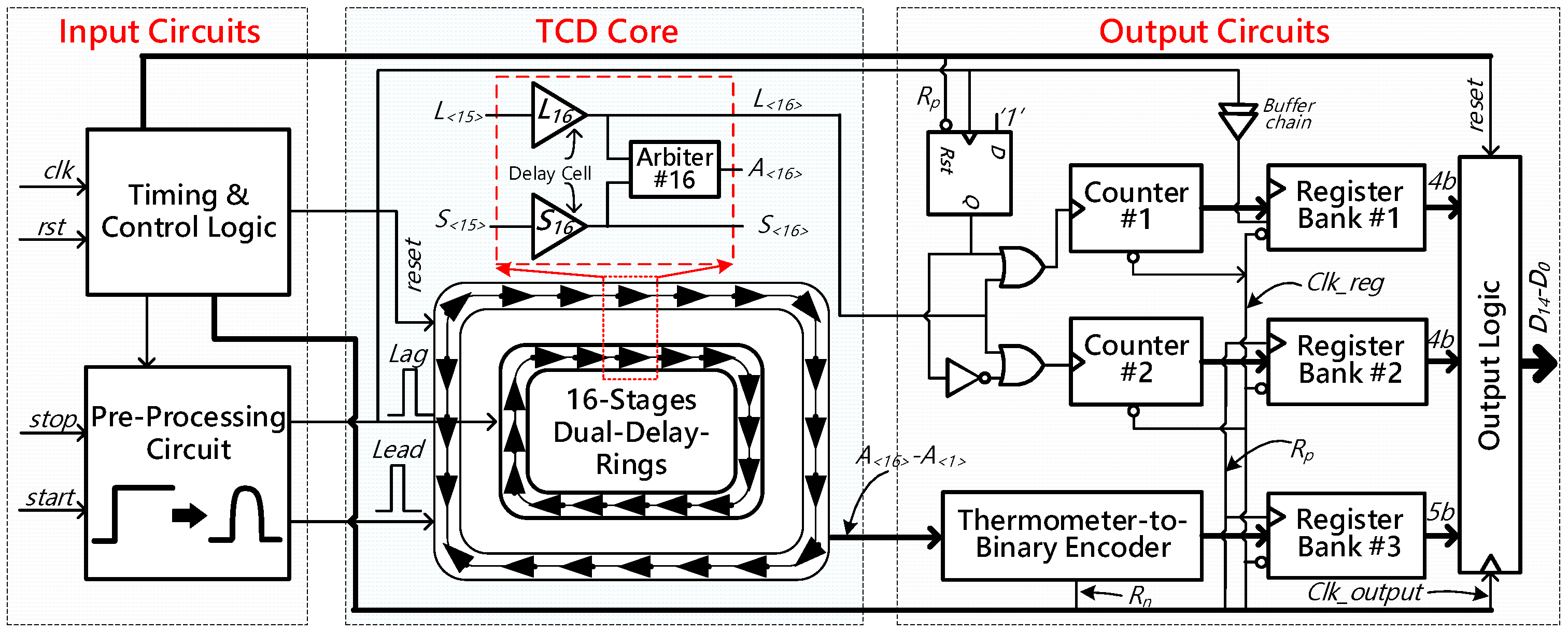
Principle block diagram of the proposed vernier time-to-digital converter (TDC).
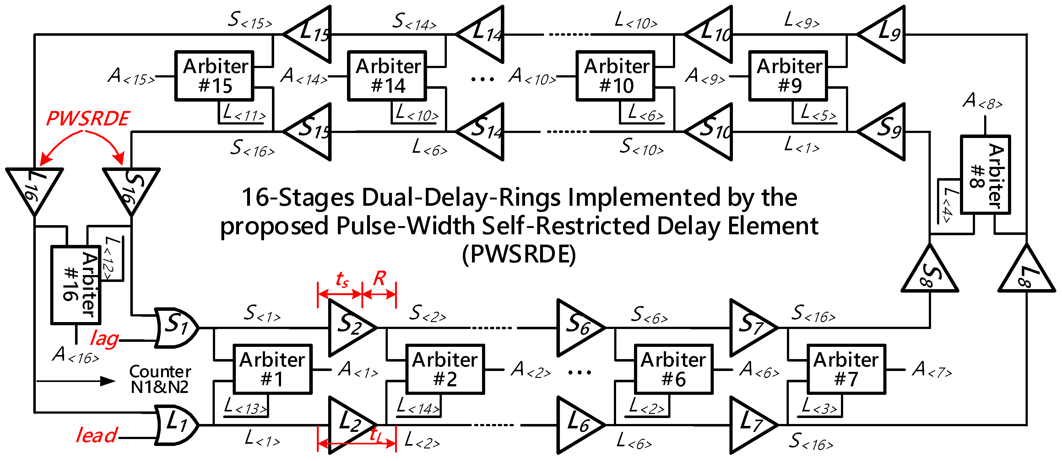
The architecture of the TDC core implemented by the 16-stages dual delay-rings.
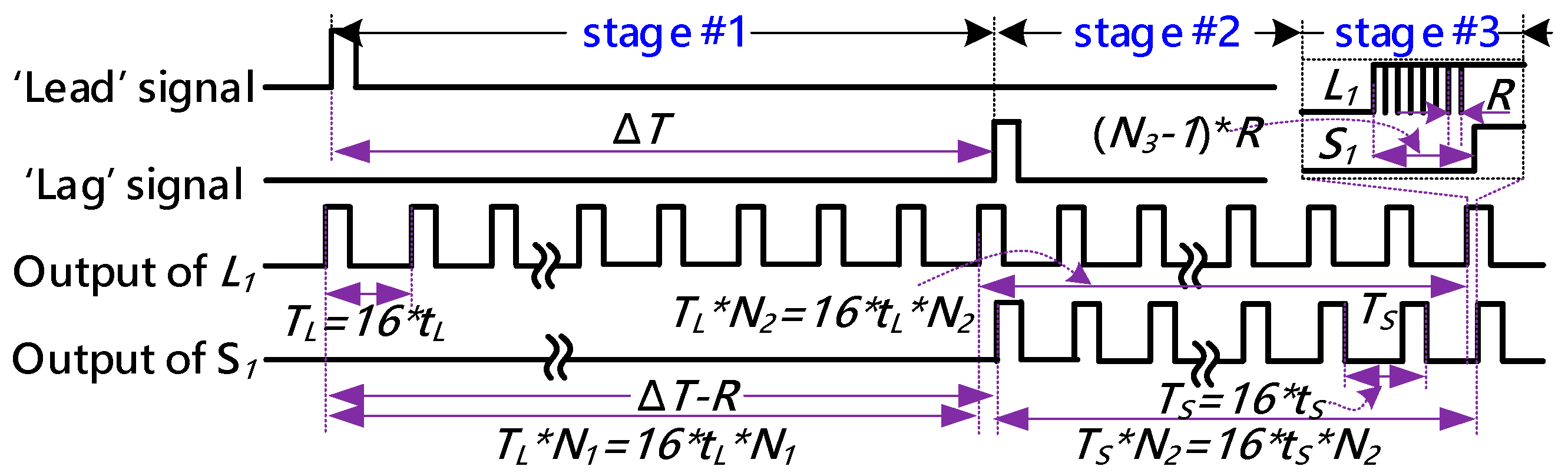
The timing diagram of the TDC core.
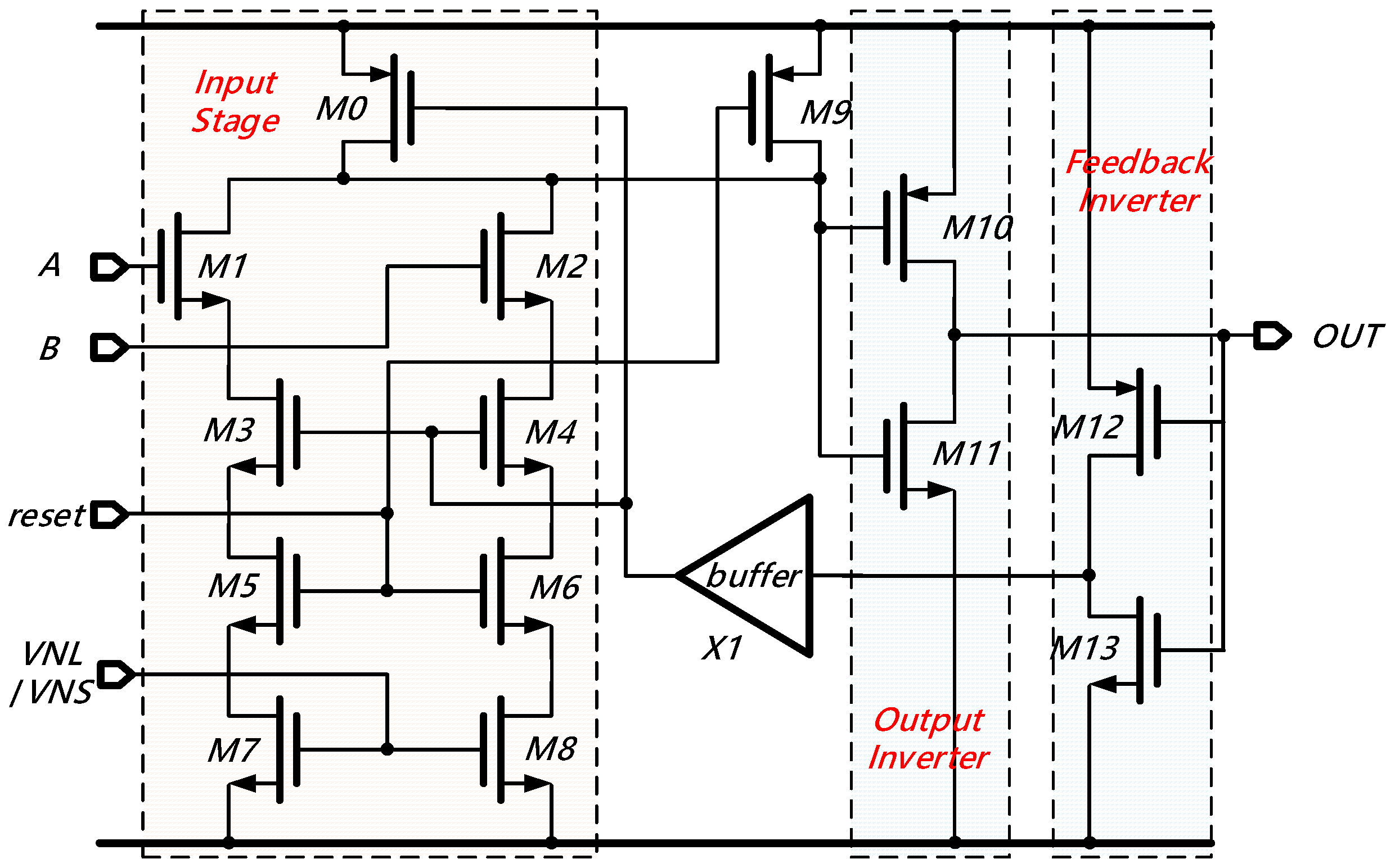
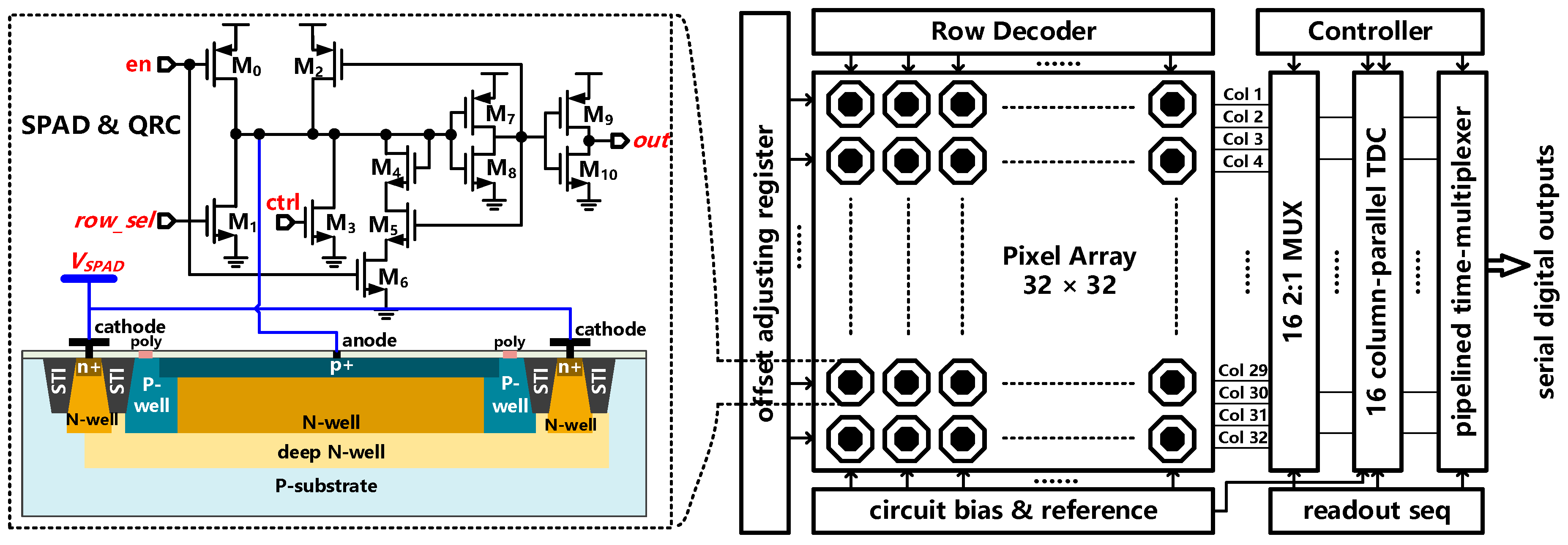
Block diagram of the 3D image sensor based on our proposed TDC (right) and its pixel circuit schematic (left).
0 Response to "12 ps resolution Vernier time-to-digital converter"
Post a Comment